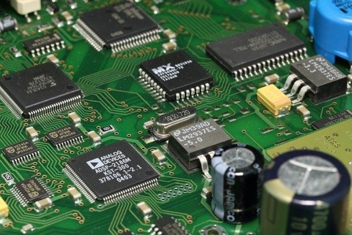
We all know PCB but majority of us don’t know types of it, we will discuss that in this article.
- We continue with our newly released PCB design section with this entry in which we will see in more detail the conductor layers on a PCB board.
- In the first introductory post we saw what a PCB is and in the previous post the parts that make up a PCB and we got a little vocabulary that we will find frequently.
- We mentioned that the “fun” of a PCB is that it has conductor tracks that “double as wires” to connect components, and that together they make an electronic circuit.
- We have also mentioned that these tracks are made using one or more layers of conductive material , usually removing parts of a continuous layer
- Now it is time to see in greater depth all this of the conductor layers . That seems like a headache but, as we anticipated, it is much easier than it seems.
- The layers make up the internal (and external) structure of the PCB. And this can be very simple or become really complex. But let’s go from less to more, looking at the simplest case, which is the case of a single conductor layer.
Table of Contents
Single Layer PCB
- We start with the structure of a single layer PCB, so called because it has a single outer layer of copper .
- Where the substrate, the copper layer, and the lacquer layer (Solder mask) have been represented. You will find similar representations in PCB design programs and manufacturers pages to represent the internal structure of the PCB that we are going to design or buy.
- However, in the manufacturing process of the PCB, part of the copper layer is removed to configure the circuit tracks and, later, the Solder mask would be applied. So really a more accurate representation of the final PCB would be something like this .
- Here part of the Solder mask is applied on the copper and part directly on the substrate. That is why you will see two shades of green (or whatever color it is), on the plates, the clearest being where there is copper underneath.
- The thickness of the substrate is usually between 0.8 and 1.6mm . There are several possible materials, the usual being fiberglass with an epoxy resin. The technology is so advanced these days.
- You will often see the designation FR4 to refer to the substrate . This does not name the material itself, but rather that it meets a NEMA standard, and indicates that it is Flame Resistant.
Two Layer PCB
- If instead of having copper on one side of the substrate, we have layers of copper on both sides of the substrate.
- Having two layers has the obvious advantage of having twice the surface area, because we have two faces to make circuits. Which translates to a smaller PCB for the same electrical circuit .
- But the biggest advantage is that with two layers we can avoid crossing . Imagine the following example, where four points have to connect with four others, but the two in the middle are “crossed”.
- If we cannot get out of the gray area (because it is full of other components) we cannot make the circuit because two tracks intersect. But if we have two layers, we can pass one of the tracks underneath (blue) and save the crossing .
- It can be shown that with two layers we can make any type of circuit, as long as we have enough surface. Something that, with a cape, is not possible, so they are very limited.
- In general, two-layer PCBs are the most common type of boards . Online services charge you the same for one of a layer as for one of two, so we will always take the two.
PCB With More Than Two Layers
- Finally and finishing, there are PCBs with many more layers. There are 4, 8, 16, up to 64 layer PCB formats. For this, the additional layers are internal layers , within intermediate substrate layers.
- Intermediate layers are usually less thick than the outer layers . In addition, they can withstand less currents because they dissipate heat worse.
- Having more layers allows very complex circuits to be made in a much smaller space . However, its design and manufacture is also considerably more complex.
- However, at the moment, PCBs with more than two layers are substantially more expensive than those with two layers. Therefore, we will focus on the two-layered, and leave the more layered for the industry (or wait a few years, to see if one day they become cheaper).
Conclusion
- So far what this entry about layers and internal constitution of the PCB. What has not been so difficult?
- Now it is worth asking: And how do we connect one conductor layer with another? That is what we will see in the next post where we will see the tracks, an essential element in almost any PCB.

